We offer research in the following areas:
Our research equipment:

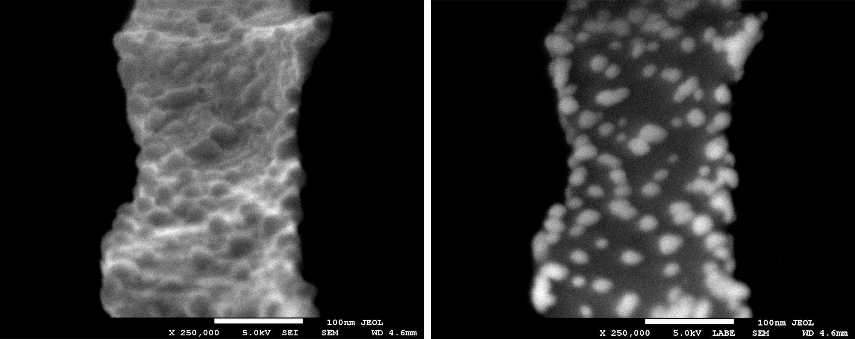
The microscope JEOL JSM-7600F is a high-resolution instrument of the latest generation, digitally controlled and equipped with an electron gun with field emission (Schottky type), which enables testing of the morphology of the surface of solids on a micro and nanometre scale. The microscope is equipped with 2 detectors for secondary electrons and 2 detectors for backscattered electrons (typical semi-conductor detector BSE and low angle backscattered electron (LABE) detector), which enable imaging of atomic contrast and differences in material density with high sensitivity. The microscope is coupled with an energy dispersion X-ray (EDX) spectrometer which enable quick analysis of the elemental compositions in solids.
The microscope is used for testing the morphology and topography of nanostructured carbon layers with added nanocrystals of transition metals and carbon nanotubes as well as for testing new materials and the results of modifications of their surface at the nano-level. The microscope is also used for solder joints, the quality of solders and intermetallic compounds in solders as well as paths in printed circuits where the scanning electron microscope with the X-ray microanalysis (EDX) module enables quick performance of qualitative and quantitative analyses.
Basic parameters of microscope:
Basic parameters of the EDX spectrometer:
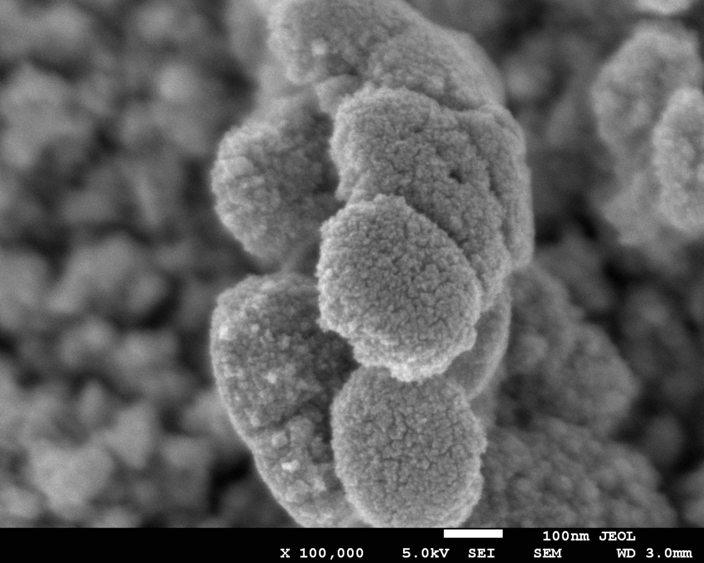
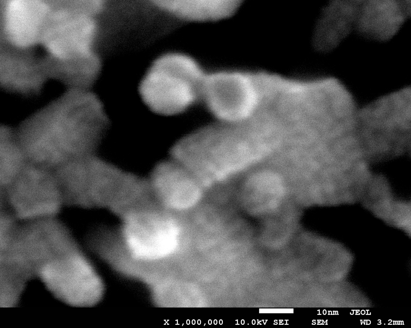
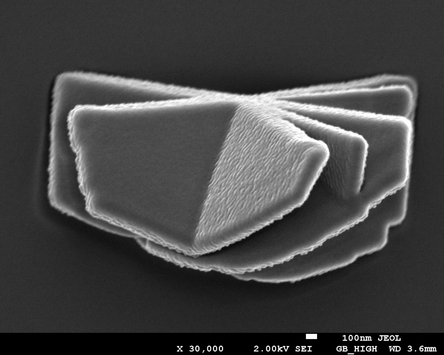
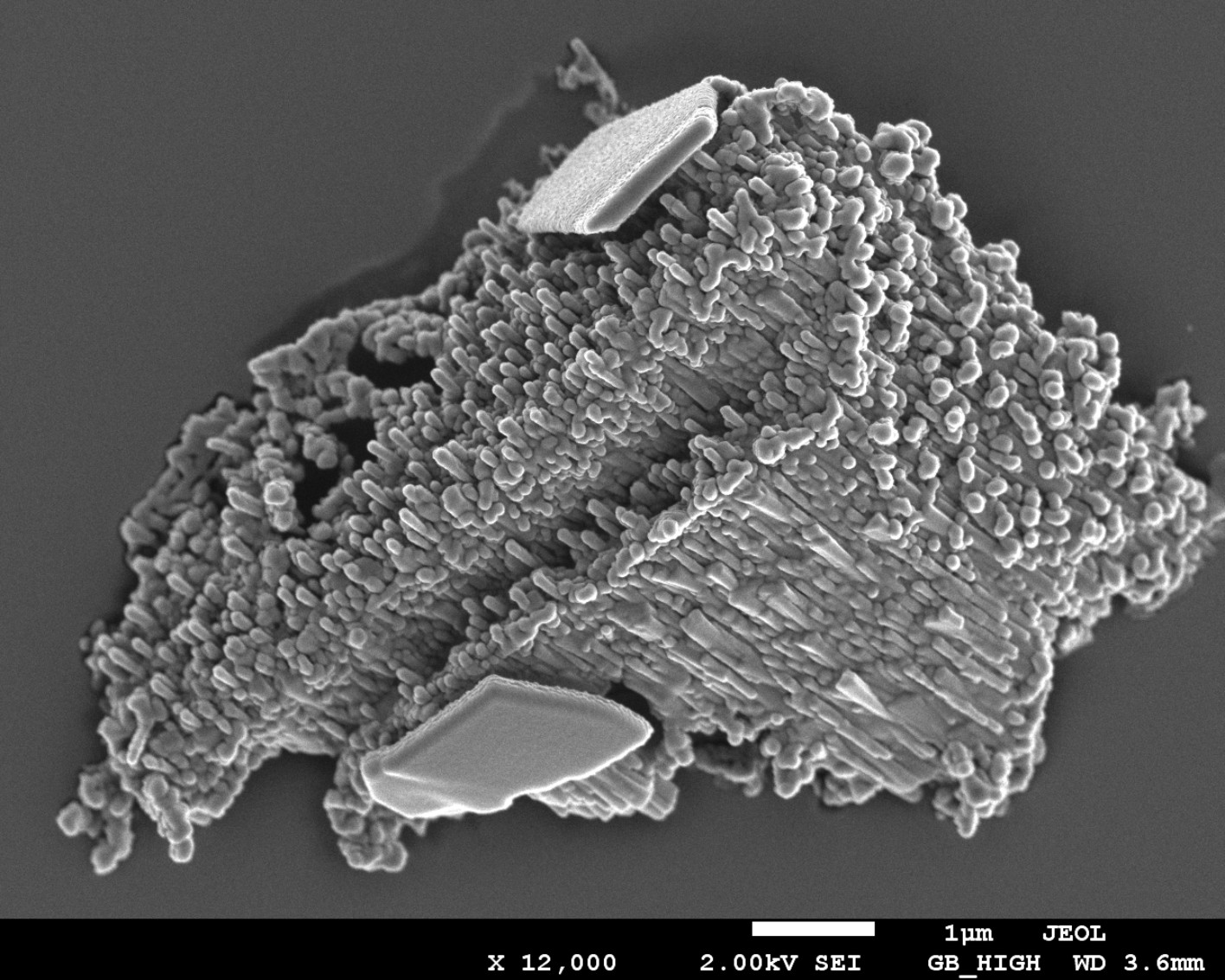
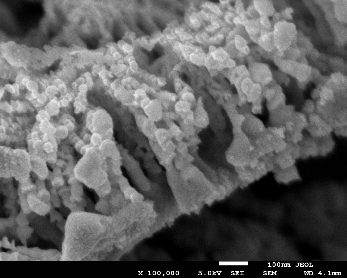
SEM images of nanostructured carbonaceous layers


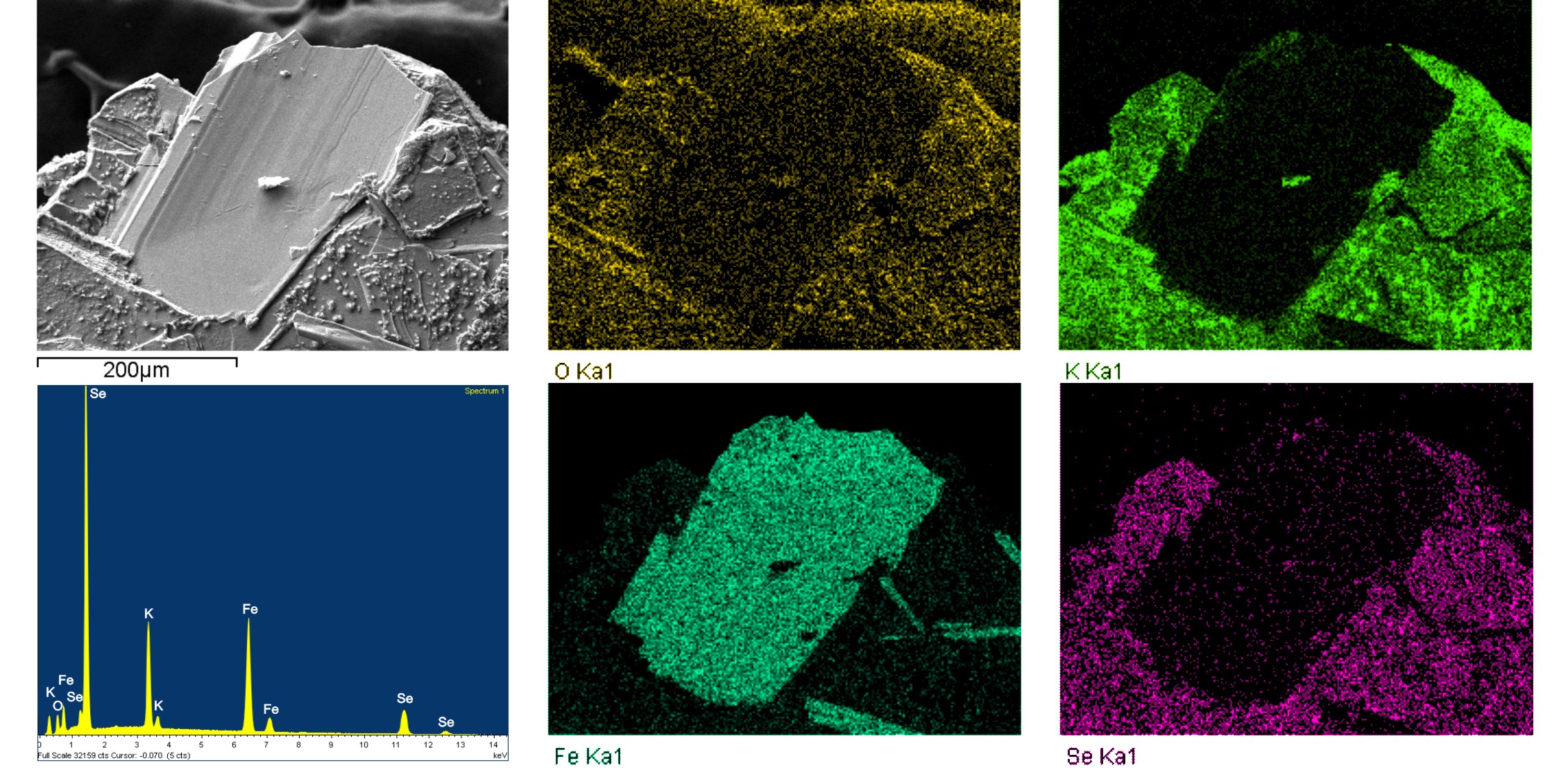
K-Fe-Se-Ocalloy surface, EDX spectrum and maps of elements